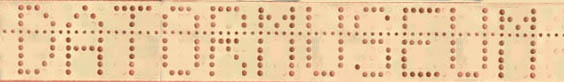
DEC VT50 series 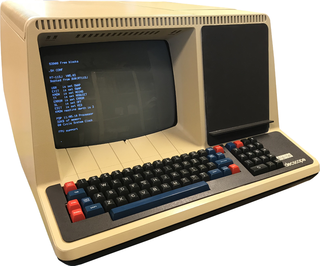 The VT50 series was a successor to the first DEC-made glass TTY, the VT05. The VT50 was announced in 1974 and provided 12 lines of 80 column text. It handled a limited set of control sequences to position the cursor etc. The VT50 was soon followed by the VT52 which handled 24 lines of text by doubling the bult in memory. The VT55 provided simple graphics drawing by adding another board inside the terminal. The VT61 and VT62 also had the same exterior but were block mode terminals. VT78 included a Intersil CMOS HM6100 based PDP-8 compatible computer inside. There were an option of having an internal photo-copier to make a screen copy on paper. The VT50 only had current loop interface while VT52 and onwards had a small replaceable module that could either be EIA RS-232 or current loop. Our VT50  We received a VT50 terminal that has been stored in an attic for the past 20+ years. The condition was good but a few screws were missing. Together with the terminal we also got the VT50 field maintenance print set. However, when the restoration was started it was soon discovered that the this VT50 had been upgraded to VT52. Both the logic board on the bottom of the terminal had been replaced with VT52 boards. VT52 is a quite simple design. The maintenance manual and print set describes it quite well, but not at all with the detail of the VT100 maintenance manual though. The logic of the terminal is splited into one UART and timing board and one data path board. 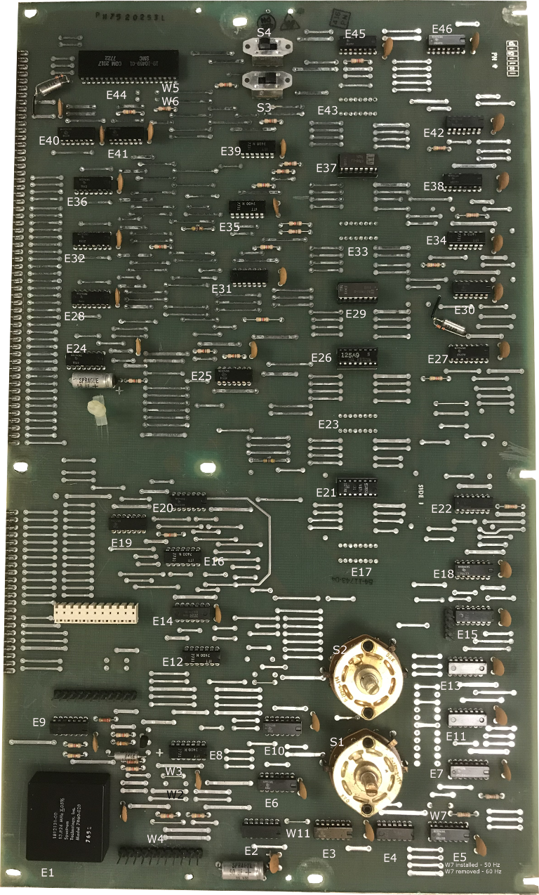 Jumper W7 controls the 50Hz of 60 Hz mode. To be installed for 50 Hz operation. If this is set wrong the picture will be waving slightly vertically which is annoying. E21, E26, E29 and E37 is the contains the microprogram of the terminal. The contents of those bipolar PROMs, 23-124A9, 23-125A9, 23-126A9 and 23-127A9 has been dumped. The UART and timing board has four 512 by 4 bipolar PROMs for a total of 1024 bytes of micro code instruction memory.
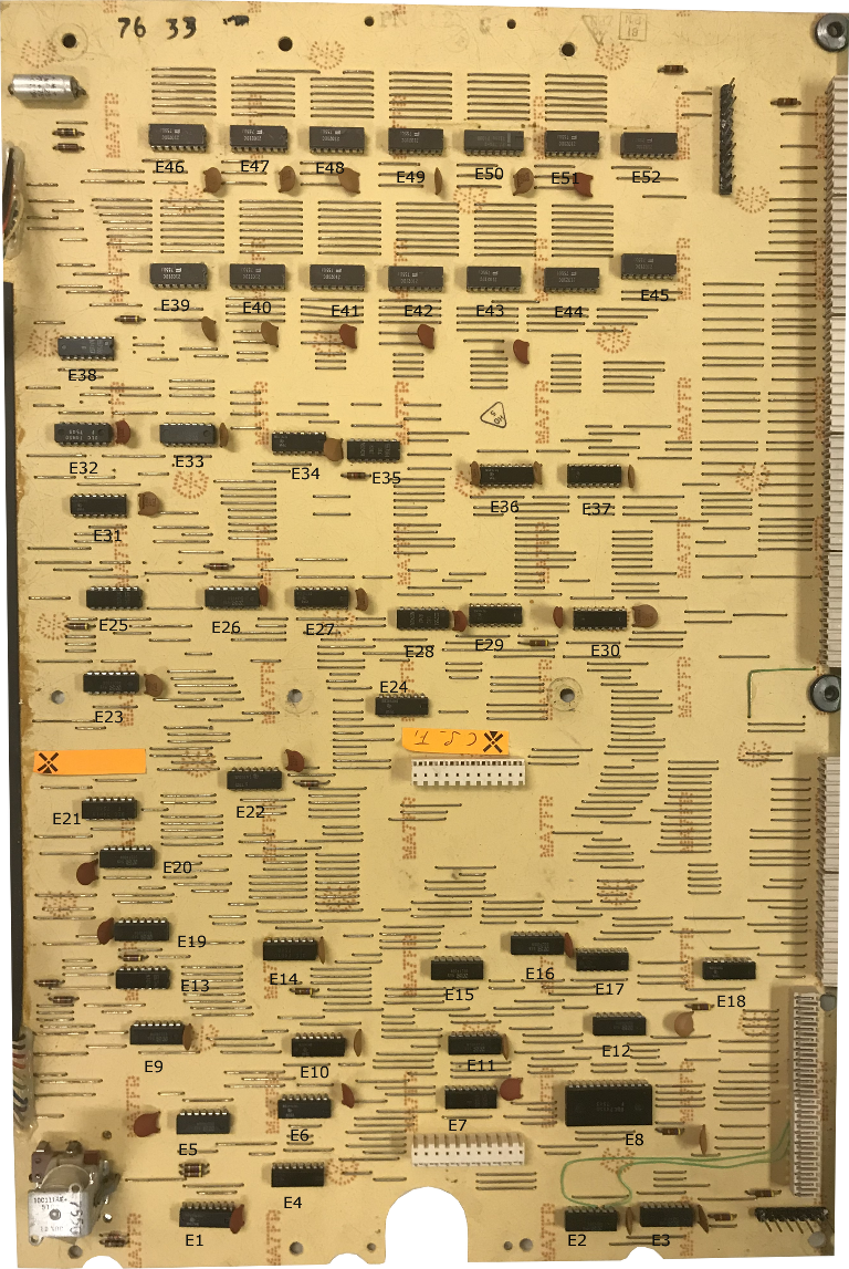 There are unfortunately nothing in the print set that indicate which component goes where on the data path board as well as no list of components, which is a great pain when debugging this terminal. I have tried to ease the apin a bit by marking the IC locations on the picture above as well as listing all components below.
VT52 instruction set. 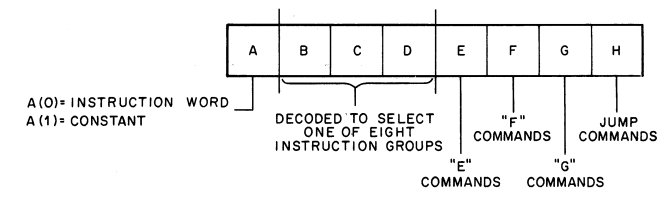 Much like the OPR class of instructions of the PDP-8 computer the four instructions of the same class can be combined simultaneously since the are executed at different points in time in the instruction cycle. 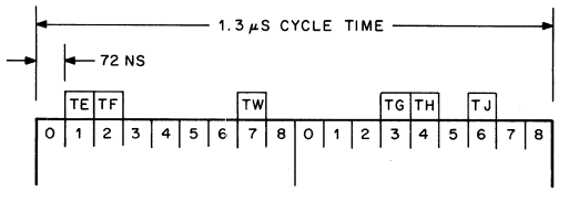 E commands are executed in TE, F commands in TF, G commands in TG and JUMP commands in TJ. Instructions with EFGH = "0000" are executed in TW and PC is incremented at TH. The 8 bit instructions are:
Microcode disassembly I thought it could be interesting to understand in more detail how the microcode of the VT52 was working and thus built a small disassembler that took the PROM files dumped and produced a disassembly list. This list is still work in progress because the actual mode of the processor affect which jump instruction to decode. The disassembler does not take this into account which means the could has to be run to get the actual mode. The disassembly program also contained a very crude simulator that allowed to trace the execution of the code in more detail. Next step is to analyze actual execution by a logic analyzer. Debugging the terminal Below is a picture showing the terminal when the repair was completed. Instead of reassembling everything and then finding out that something was more was broken, disassemble everything, fix it and repeat, I decided to do most parts of the testing on the bench. 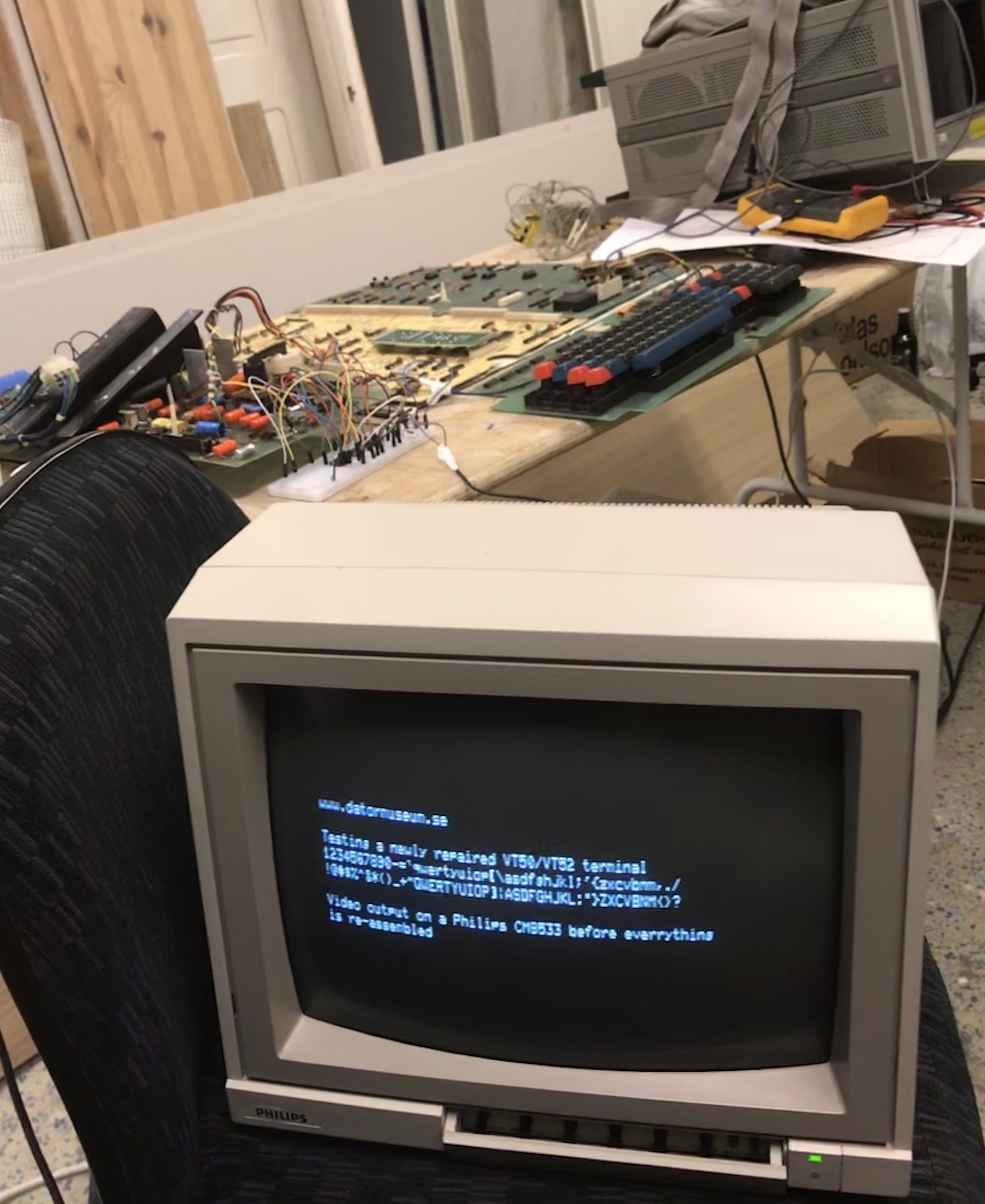 To ease the debugging effort the PSU, Keyboard, UART and timing board and data-path board were laid out flat on a table. One electrolytic capacitors shown minor leaking. To be able to run the terminal without generating any HV a jumper was lifted on the power supply / monitor board. 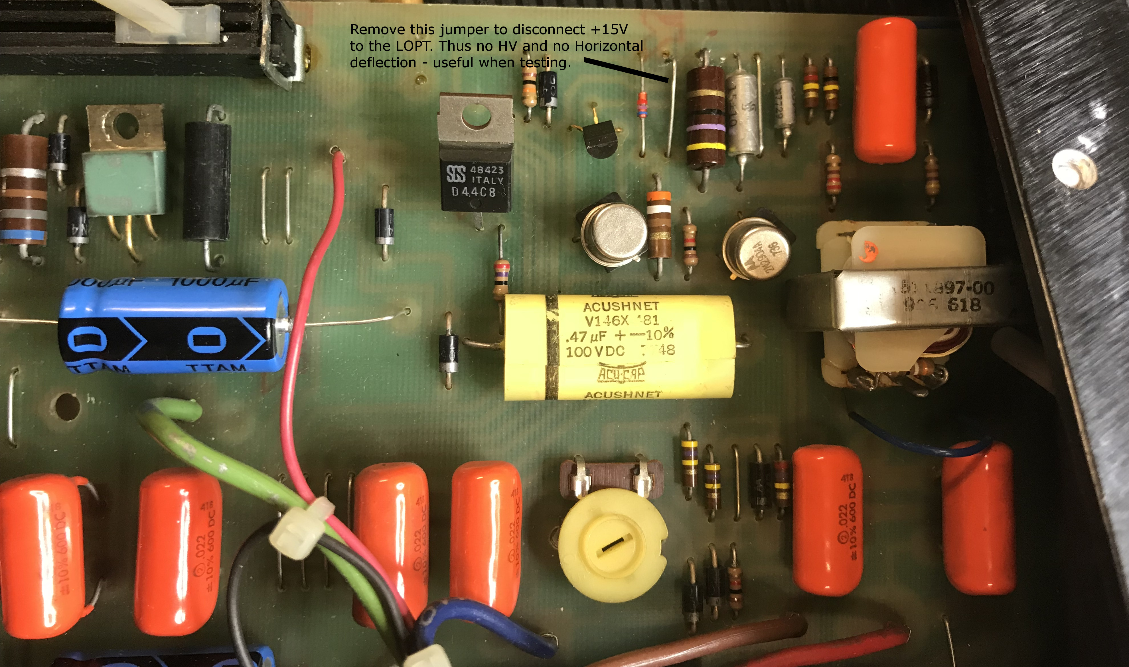 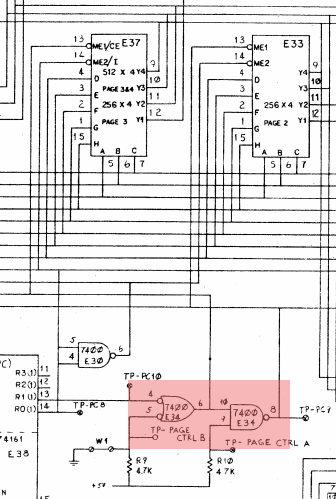 Probing with the scope gave that the chip enable inputs for every single bipolar PROM was high. Thus inactive! That cannot be correct. The chip enable signals were generated by 7400 NAND get E34 and when probing the output of one of the gate it showed a very suspicious 2V level at the output. This is not normal since 2V is on the very threshold for a TTL circuit. Normally this means that the output pin is open circuit and nothing is driving it. The reason for having 2V there is that input circuit of the next gate is driving it to this potential. Changing E34 for a new chip gave much more activity on the PROM output lines. But still no key click unfortunately. While probing around for potential faults I found another ITT made 7400 NAND gate that showed exactly the same behaviour as this gate. This time it was the cursor flip-flop E8 that was bad. 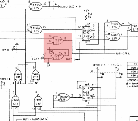 Unfortunately this still didn't mean complete success. Still no key click when pressing the keys on the keyboard. Other fellow VT52 terminal repairers on the cctalk mailing list suggested that the IC sockets for the bipolar PROMs had gone bad. Not uncommon for old socket to get too oxidized. And actually pulling out and re-inserting the PROM chips eventually gave a proper key click. Decision was made to completely replace all the sockets and the terminal was in much better mode. Probing the video signal output showed a signal. But was it all right? Hard to tell without the monitor attached. There could be all sorts of problems in the datapath board that could give corrupted video. So how could it be tested without the display connected. By using a standard composite video monitor of course! By looking at the schematics for the VT100 terminal I came up with a quick and dirty circuit that solved the problem. A small bread board mock up was constructed and soldered into place and a Philips CM8533 monitor was attached. Yes, indeed! The terminal did work! 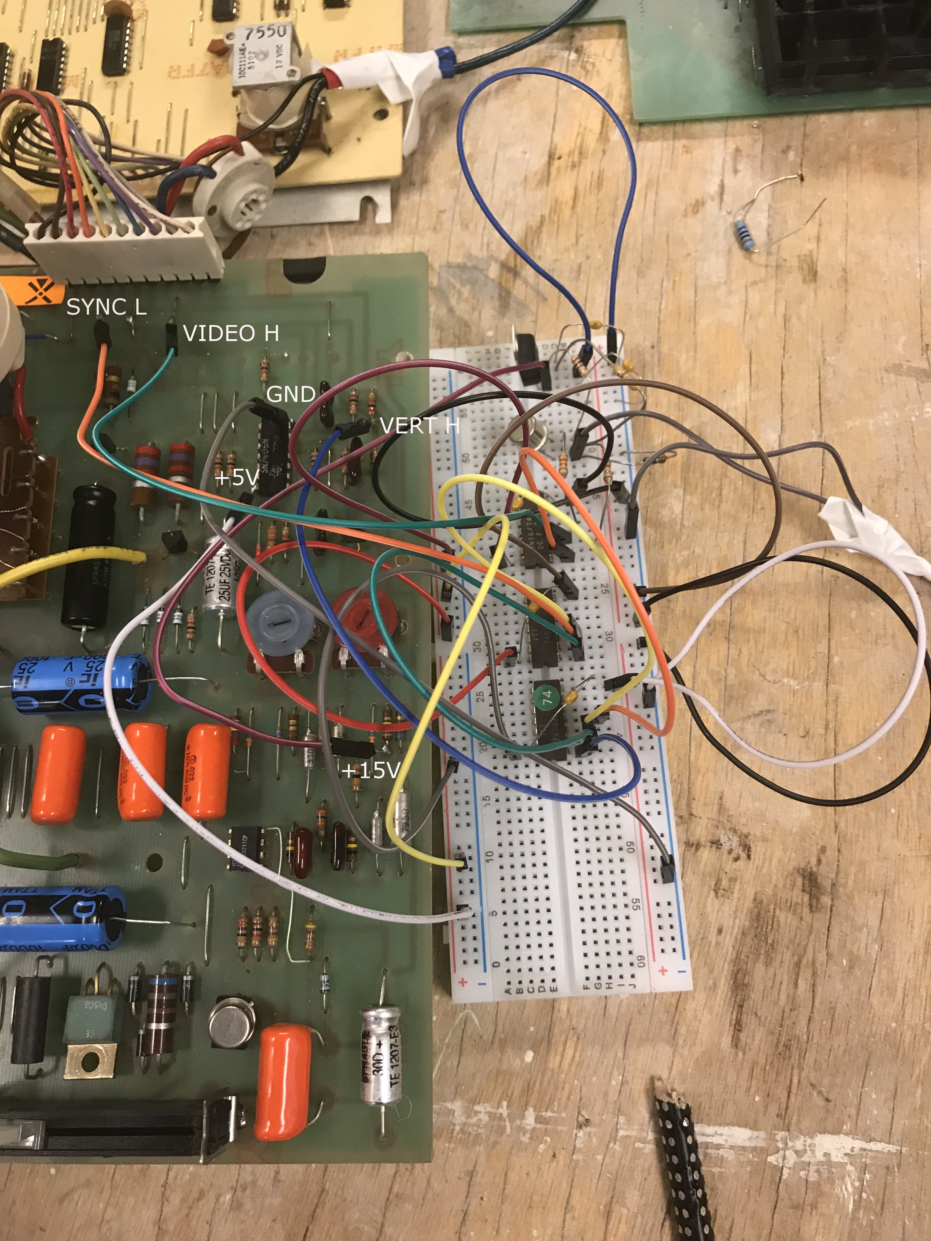 And here is a quick schematics for the circuit above in case anyone has a need for it (or myself in the future). 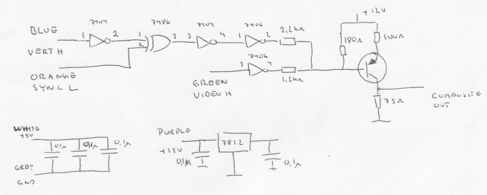 Apart from that a bad solder joint on a small pulse transformer in the LOPT drive circuit the terminal worked fine and could be reassembled. |
Home >